There are six common PCB depaneling methods used in the electronics manufacturing industry:
V-CUT Depaneling (Blade / V-Groove Depaneling)
Router Depaneling (CNC Routing)
Laser Depaneling
Punching Depaneling
Saw Depaneling
Manual Depaneling (Breaking / Cutting by Hand)
Currently, the most widely used methods in electronics manufacturing are:
V-CUT Depaneling
Punching Depaneling
Router Depaneling
Saw Depaneling
Laser Depaneling
Since PCB structures, materials, component spacing, stress requirements, and production capacity vary from product to product, manufacturers need to choose the most suitable depaneling method based on their specific applications.
Many manufacturers focus heavily on SMT, AOI, and testing processes, while often overlooking PCB depaneling.
In reality, improper depaneling can directly lead to:
Solder joint micro-cracks
Component detachment
Board edge cracking
PCB deformation
FPC burn marks
Lower production yield
Increased customer complaints
This issue is especially critical in industries such as:
AI servers
Automotive electronics
Energy storage BMS systems
Medical electronics
Optical modules
Wearable devices
Consumer electronics
As PCB designs become increasingly complex, depaneling requirements continue to rise.
According to reliability studies published by IPC:
PCB depaneling defects account for approximately 5%–15% of total manufacturing defects
In high-precision PCBA products, hidden damage caused by depaneling can exceed 20%
Micro-crack issues are often discovered only after products are shipped
According to case studies from SMTA:
If depaneling stress is not properly controlled:
Overall repair costs may increase by 8%–30%
This is particularly important for new energy vehicles and wearable electronics, where low-stress depaneling is becoming a critical requirement.
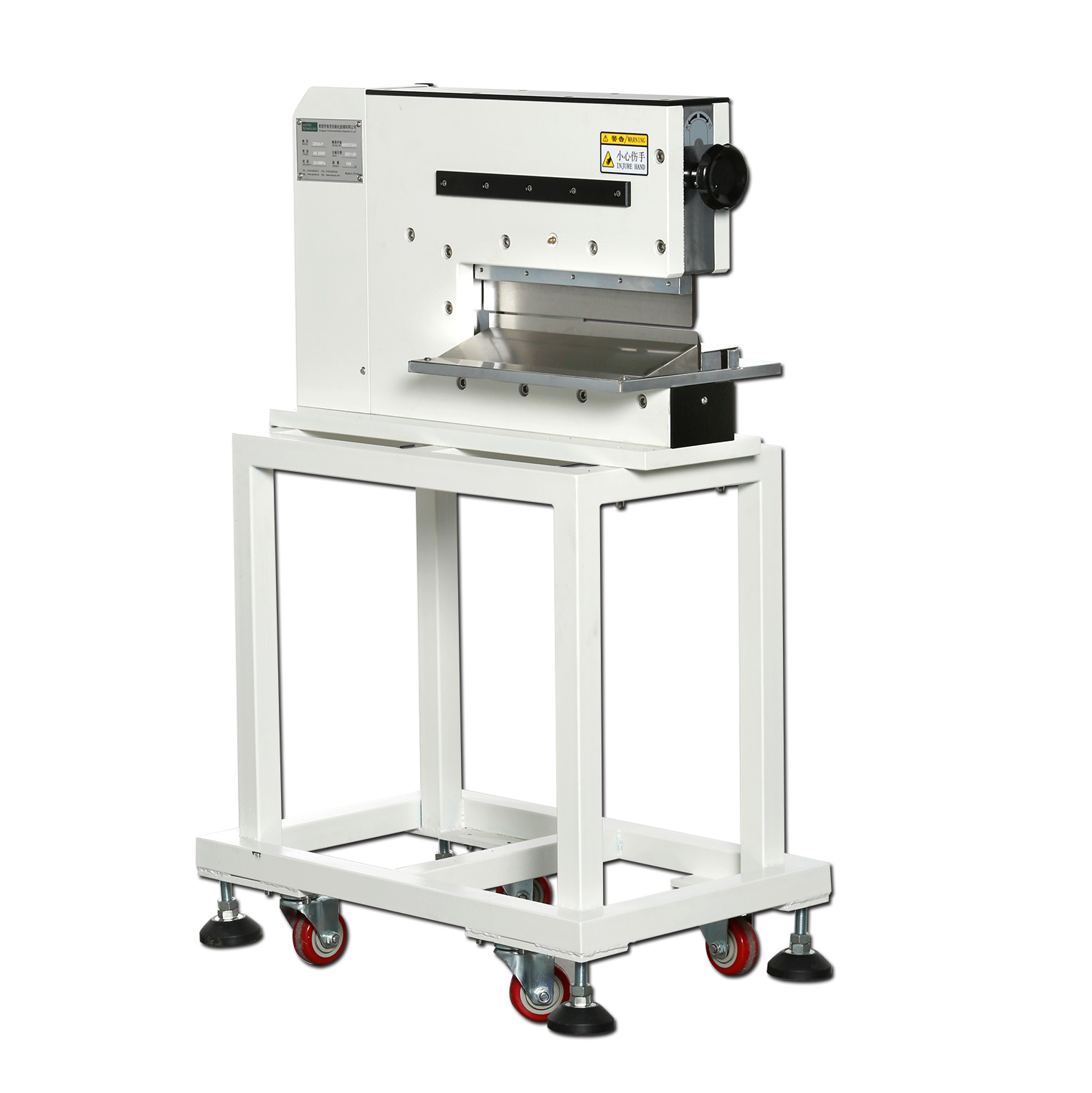
V-grooves are pre-scored on the PCB panel, and upper/lower circular blades separate the boards.
Low cost
High speed
Lower equipment investment
Ideal for mass production
Higher mechanical stress
May damage components near board edges
Not suitable for irregular-shaped boards
LED boards
Power supply boards
Home appliance control boards
Standard consumer electronics PCBs
A high-speed spindle drives the routing bit to cut connection points along a programmed path.
Lower stress
Suitable for irregular board shapes
High precision
Widely used
Tool wear costs
Requires effective dust collection
Slower than V-CUT
Smartphone motherboards
Automotive electronics
Industrial control products
Communication modules
GAM330
GAM320A
GAM336AT
GAM330AT
GAM386AT
ZM300 Series
Suitable for automated inline production.
Uses UV laser or CO₂ laser technology for non-contact cutting.
No mechanical stress
High precision
No tool wear
Suitable for PCB, FPC, and rigid-flex boards
Higher equipment investment
Requires precise parameter tuning
AI smart glasses
Medical electronics
Flexible circuits
Camera modules
TWS earbuds
Offline laser depaneling machines
Inline automated laser depaneling systems
Uses custom molds to separate boards in a single punching action.
Extremely fast
Low operating cost
Ideal for ultra-high-volume production
High mold costs
Low flexibility
Higher mechanical stress
LED boards
Small consumer electronics
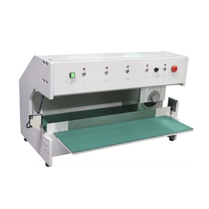
Uses high-speed saw blades for straight-line cutting.
High cutting efficiency
Clean cutting edges
Lower stress
Only suitable for straight cuts
Not suitable for complex irregular boards
Aluminum PCBs
Long strip PCBs
LED boards
ZM300SV
ZM336ASV
ZM300H
Operators manually break boards apart or use simple hand tools.
Lowest cost
Highest risk
Low yield
Not suitable for large-scale production
This method is gradually being phased out by professional electronics manufacturers.
You can evaluate based on these six factors:
FR4
FPC
Aluminum PCB
Ceramic PCB
If components are located less than 1mm from the board edge, prioritize:
Router Depaneling
Laser Depaneling
High-value products typically require low-stress depaneling methods.
Examples include:
Automotive electronics
Medical electronics
Optical modules
For irregular-shaped boards, choose:
Router Depaneling
Laser Depaneling
For ultra-high-volume production:
Punching
V-CUT
With the rise of smart factories:
Demand for inline automated depaneling equipment continues to grow rapidly.
According to reports from Prismark Partners LLC:
From 2025–2028:
EV PCB demand will continue growing
AI server PCB demand will rise
High-frequency/high-speed PCB demand will expand
This growth is driving demand for:
Laser depaneling
High-precision router depaneling
Automated depaneling systems
With over 30 years of experience in PCB/FPC depaneling, Genitec/ Seprays provides:
Router depaneling machines
Laser depaneling machines
Saw depaneling machines
Punching depaneling machines
Inline automated depaneling production lines
Automatic unloading and tray loading systems
Serving industries such as:
Consumer electronics
Automotive electronics
New energy
Medical electronics
Communications
Traditional V-CUT caused solder joint cracking.
Implemented Seprays/Genitec router depaneling solution.
Scrap rate significantly reduced
Yield improved
Severe edge burning during FPC cutting.
Adopted Seprays/Genitec laser depaneling solution.
Improved cutting precision and achieved stable mass production.
Insufficient production capacity.
Implemented Seprays/Genitec inline saw depaneling solution.
Production capacity increased by 35%
There is no universally “best” method—only the most suitable one for your product structure.
Not when parameters are properly optimized.
For high-precision stamp-hole panel designs, router depaneling is recommended. For standard V-groove panel designs, V-CUT is often sufficient.
For high precision and premium quality, laser depaneling is recommended.
For lower quality requirements with very high production volume, punching may be suitable.
Low-stress, high-reliability router or laser depaneling is recommended.
PCB depaneling is evolving from traditional rough processing toward:
Higher precision, lower stress, greater automation, and smarter manufacturing.
Choosing the wrong depaneling method can directly impact product yield and profitability.
Choosing the right equipment can significantly improve your competitiveness.
Contact Seprays/ Genitec for:
✅ Free sample testing
✅ Depaneling process evaluation
✅ Automation solution recommendations
✅ Industry case references
Visit: dg-genitec.com、sales@genitec.tw
Make depaneling more stable. Make manufacturing more efficient.