Micro-Stress PCB Depaneling Solutions for Wearable Devices
Low-Stress Milling Technology for High-Precision PCBA
H1: Micro-Stress PCB Depaneling for Wearable Electronics
Wearable electronics such as smartwatches, TWS earbuds, smart bands, and medical patches place exceptionally high demands on PCB depaneling processes.
Typical PCB characteristics include:
Ultra-thin board thickness (0.4–1.0 mm)
Small form factor with complex outlines
High component density, often close to board edges
High-value, high-precision PCBA assemblies
If stress is not properly controlled during depaneling, the following risks may occur:
Micro-cracks in solder joints
Pad lifting
Substrate cracking
Component failure
Latent reliability risks leading to high field repair rates
For this reason, micro-stress depaneling has become a critical control parameter in wearable PCB manufacturing.
H2: Why Milling Depaneling Is the Optimal Solution for Wearables
Compared with stamping, V-cut, blade routing, or saw depaneling methods, PCB milling offers:
Lower cutting stress
Smooth, burr-free edges
Excellent adaptability to irregular shapes
High cutting precision
Stable support through dedicated fixtures
In large-scale SMT production validation, low-stress milling solutions significantly reduce latent defect risks and improve overall yield rates.
H2: Why Milling Is More Suitable for Wearable PCBs
1️⃣ Superior Stress Control Capability
Wearable products feature highly compact layouts. Solder joints are extremely sensitive to strain.
Excessive stress may cause:
BGA solder ball cracking
Trace damage
Capacitor failure
Micro-fractures in substrates
Milling depaneling uses a high-speed spindle cutting process, delivering more uniform stress distribution and avoiding sudden mechanical shock.
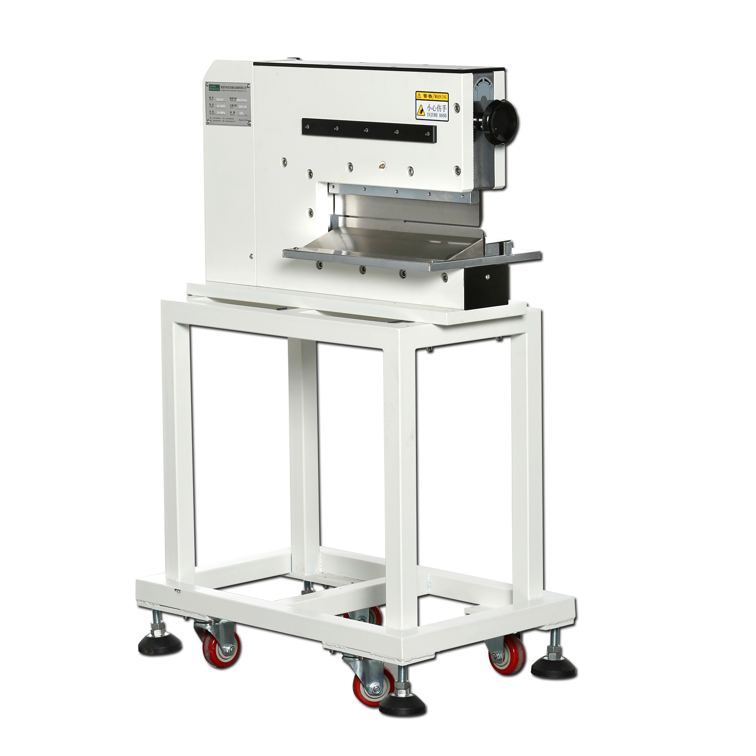
Taking the GAM330 Series from Dongguan Seprays / Genitec Automation Equipment Co., Ltd. as an example:
Imported high-speed spindle up to 100,000 rpm
Reduced cutting stress
Smooth board edges
High repeatability accuracy
Integrated Z-axis suspension structure to prevent offset
(Data source: GAM330 technical documentation)
2️⃣ Core Micro-Stress Control Structures
Effective micro-stress control relies on three structural elements:
✔ Floating Brush Mechanism
Patented floating brush design minimizes Z-axis impact during cutting.
✔ High-Precision Spindle System
High-speed precision spindle reduces vibration and mechanical runout.
✔ Dedicated Fixture Support
Custom fixtures provide superior thin-board support compared to universal fixtures, minimizing deformation.
Together, these elements keep depaneling stress within acceptable limits for wearable PCBA assemblies.
3️⃣ Dust and ESD Control: Equally Critical
Wearable devices are used in close-contact environments and require exceptional reliability.
Potential risks include:
Conductive dust causing short circuits
Hygroscopic dust leading to intermittent failures
ESD damage to sensitive components
The GAM330 Series integrates:
Upper and lower high-velocity dust extraction system
HEPA filtration
Negative pressure monitoring
ESD-safe spindle
Static eliminator (reduces 1000V to 100V within 1 second)
For high-value wearable boards, dust and electrostatic control are essential safeguards for yield protection.
H2: Recommended Solution Configuration
Recommended Equipment:
GAM330
GAM330L
GAM330X
Dual-spindle version (for high-throughput production)
Suggested Core Configuration:
| Item | Recommended Configuration |
|---|---|
| Spindle | High-speed precision spindle (100,000 rpm) |
| Fixture | Custom dedicated fixture |
| Dust Collection | Dual upper & lower extraction + HEPA |
| ESD Protection | Anti-static spindle + static eliminator |
| Vision System | CCD automatic compensation alignment |
The dual-working-table design enables:
Depaneling on one side
Loading/unloading on the other side
This increases equipment utilization by approximately 30%, validated in mass production environments.
H2: Application Scenarios
Seprays / Genitec milling depaneling solutions are widely applied in:
Smartwatch PCBA
TWS earbud mainboards
Medical patch boards
IoT mini modules
High-end consumer electronics
Long-term customers include:
OPPO
Foxconn
Luxshare Precision
Quanta Computer
Bosch
(Partial customer list; based on application case data)
H2: Why Choose Seprays / Genitec?
Established in 1993 with over 30 years of PCB depaneling expertise
Self-developed software with lifetime free upgrades
180+ patented technologies
Service support across 31 countries
Industry top-three market share
Seprays / Genitec’s competitive strength in wearable micro-stress depaneling lies not only in equipment structure, but also in:
Structural stability
Mature control software
Comprehensive dust management system
Long-term mass production validation experience
For high-value, ultra-thin, small-form-factor wearable PCBA, process stability is far more critical than initial equipment cost.
FAQ
Q1: Why must depaneling stress be controlled for wearable PCBs?
Thin substrates combined with densely packed components are highly strain-sensitive, making them prone to latent solder joint cracks.
Q2: Is V-cut depaneling suitable for wearable products?
Not recommended. V-cut relies on mechanical fracture, causing concentrated instantaneous stress that is unsuitable for thin, high-density boards.
Q3: Does milling depaneling generate dust?
Yes, but an efficient dust extraction system effectively controls contamination and mitigates quality risks.
Q4: Is a dual-spindle system necessary?
For high production volumes, dual-spindle configurations can improve efficiency by approximately 30%.
Conclusion
As wearable devices continue evolving toward lighter, thinner, and more compact designs with higher reliability requirements, PCB depaneling has transitioned from simple separation to micro-stress engineering control.
Selecting a mature and stable milling depaneling solution is a critical step in ensuring long-term product reliability.
The GAM330 Series low-stress high-precision depaneling machines have been validated across numerous high-end electronic manufacturing environments and represent a preferred solution for wearable PCB depaneling.
Free PCB Depaneling Solution Consultation
Seprays / Genitec provides free PCB depaneling process evaluation and solution recommendations.
Hotline: +86 139 2926 8485 E-mail:sales@genitec.tw